Week 1 HW: Final Project Ideas
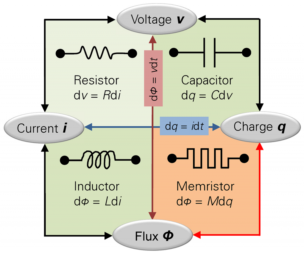
part1 My idea is to use biomanufacturing to produce materials for small memristors, assemble them into dense arrays, and evaluate their performance. The goal is to fit many functional devices into a compact circuit for potential applications in neuromorphic computing. For example, Professor Hyun Jae Kim and his colleagues at Yonsei University demonstrated a memristor array using mucin, a naturally occurring glycoprotein, showing that biological materials can support electronic behavior that resembles synaptic activity (Moon et al., 2025).
Although memristor arrays with features as small as 2 nm have already been demonstrated, manufacturing densely packed electrodes with sufficiently low electrical resistance remains a significant engineering challenge (Pi et al., 2019). Producing large arrays also requires consistent switching behavior and a high proportion of working devices, as demonstrated by research on a 4,096-device array (Kim et al., 2021). To illustrate the scale of this problem, a hypothetical array of one million devices with a 1% defect rate would contain 10,000 faulty cells.
One possible approach is to cultivate bacteria that produce protein nanowires and use the collected material in the active layer of memristors. Working memristors made using bacterial protein nanowires have already been demonstrated (Fu et al., 2020). I hypothesize that growing these nanoscale building blocks in batches could provide a scalable source of material for many devices. Precise electrode fabrication and assembly would still be necessary. I would investigate whether this approach can produce reliable arrays by measuring switching behavior, device-to-device variation, and the proportion of functional cells. The intended users would be researchers and engineers developing compact neuromorphic hardware.
If bacterial protein-nanowire devices cannot retain programmed weights for sufficiently long periods, I would investigate chemically modified silk fibroin as an alternative active material. Wang et al. (2021) demonstrated an analogue memristor based on a silk fibroin polymer with more than 32 conductance levels maintained for four months (https://doi.org/10.1039/D1TC03315H). This makes it a promising protein-based candidate for longer-term weight storage. Adopting this material would require adapting the production process and testing whether its retention and switching performance remain consistent across a larger array.
part2 I would produce protein nanowires for the active layer of a memristor. My proposed living system is a laboratory strain of Escherichia coli engineered to produce these nanowires. Researchers have already demonstrated the production of electrically conductive protein nanowires using engineered E. coli, making it a possible starting point for this project (Ueki et al., 2020: https://doi.org/10.1021/acssynbio.9b00506).
The inputs would include water, a carbon source, nitrogen, mineral nutrients, and oxygen. I would investigate growing the bacteria in a controlled bioreactor, where they would synthesize proteins and assemble them into nanowires. After cultivation, the material would be harvested and purified to separate the nanowires from bacterial cells and other components. Simply removing the bacteria from the culture medium might not recover the product, because some nanowires could remain attached to the cells.
The output of the biological process would be a purified nanowire suspension that could be produced in batches and used to fabricate many devices. This suspension would be deposited onto substrates with patterned metal electrodes and dried to form a protein film. Memristors incorporating bacterial protein nanowires have already been demonstrated (Fu et al., 2020: https://doi.org/10.1038/s41467-020-15759-y). However, I would need to verify that the engineered E. coli can produce useful quantities in liquid culture and that its purified nanowires support the required switching behavior.
part3 I would combine biological production with automated liquid handling and device fabrication. An Opentrons robot could prepare media and dilution series for comparing culture conditions and nanowire concentrations. Automating these repetitive steps would help make experiments more consistent and allow several conditions to be evaluated in parallel (Opentrons documentation: https://docs.opentrons.com/python-api/tutorial/).
For device fabrication, I would use lithography to define the electrodes and their spacing. I would then investigate automated dispensing or inkjet printing to deposit the nanowire suspension into predefined regions. Lithography would determine the small electrode gaps, while printing would deliver the biological material over larger areas. Protein nanowire films have already been used with lithographic patterning and solution deposition, although printing this particular suspension would require additional testing (Fu et al., 2020: https://doi.org/10.1038/s41467-020-15759-y).
I would complete aggressive processing steps before depositing the protein material and then use compatible drying and protective packaging. Burning away excess material could damage the functional film. Finally, an automated electrical probe station would measure device characteristics and identify defective cells. For larger production volumes, I would investigate processing multiple devices together on wafers and testing them through parallel measurement channels.
part4 My long-term motivation is to develop physical AI hardware for robotics, potentially including systems that process sensor signals for bipedal balance and walking. I would begin with approximately 1,000 working devices to evaluate their electrical behavior. For a later manufacturing scenario, I would consider producing one billion working devices across many chips. This would be a scale-up target rather than an estimate of how many devices a single robot requires.
To estimate material demand, I would use a reported deposition of 110 µL/cm² of a 150 µg/mL nanowire suspension, which produced a film approximately 1 µm thick (Fu et al., 2020: https://doi.org/10.1038/s41467-020-15759-y). This corresponds to 0.110 mL/cm² × 150 µg/mL = 16.5 µg/cm². For this calculation, I assume a 10 × 10 µm coated region per attempted device, 10% material utilization during deposition, and a 50% functional-device yield. These are planning assumptions, and the coated region does not represent the complete circuit footprint.
A 10 × 10 µm region has an area of 10⁻⁶ cm² and would therefore contain approximately 16.5 pg of nanowires. Producing one billion working devices at a 50% yield would require two billion attempted devices. Their films would contain approximately 2 × 10⁹ × 16.5 pg = 33 mg of nanowires. With only 10% of the purified material reaching the intended films, the total requirement would become 33 mg ÷ 0.10 = 330 mg.
For the prototype, I would budget a total coated area of 1 cm² across test samples, including unused regions, containing at least 2,000 attempted devices. At the assumed 50% yield, this would provide approximately 1,000 working devices. Including deposition losses, the material requirement would be 16.5 µg ÷ 0.10 = 165 µg, or 0.165 mg.
For biological production, I assume a recovered yield of 1 mg of purified nanowires per litre of culture and a three-day cultivation-and-recovery cycle. These values would need to be measured experimentally. Under these assumptions, one 1 L batch would provide enough material for the prototype. Producing 330 mg would require 330 L of culture in total. Four reactors, each with a 10 L working volume, would provide 40 mg per cycle, requiring nine cycles, or approximately 27 days. If the recovered yield were only 0.1 mg/L, the same equipment would require approximately 249 days.
Fabricating and testing the devices would require additional time. Once a prototype process was established, I would provisionally allow another one to two weeks for fabrication and testing. For the manufacturing scenario, I assume a line capable of fabricating and initially screening 10 million attempted devices per day. At a 50% yield, it would produce five million working devices per day, requiring approximately 200 production days to reach one billion. Sequential biological production and device manufacture would therefore take approximately 227 days, although overlapping the processes could reduce this. These estimates exclude initial research and process development, and the assumed manufacturing throughput would also need validation.
part5 One major unknown is the amount of usable material the bacteria can produce. I would need to measure purified nanowire yield per litre, losses during separation and purification, and variation between batches. These results would determine whether my assumptions about production time and reactor capacity are realistic.
Another challenge is producing uniform films and reliable electrical contacts. Nanowires could aggregate, deposit unevenly, or become damaged during processing. I would measure their dimensions, film thickness, surface coverage, and the proportion of working devices. Because this approach uses a film, I would first investigate whether alignment and length variation affect performance before assuming that every wire must be positioned individually.
The third unknown is whether these devices would support the type of computation I want to perform. The protein nanowire memristors demonstrated by Fu et al. have volatile switching, meaning their conductive state relaxes over time (Fu et al., 2020: https://doi.org/10.1038/s41467-020-15759-y). This could be useful for neuron-like dynamics, while persistent neural-network weights would require additional memory or a different device design. I would evaluate switching voltage, state lifetime, endurance, and energy use before testing a small sensor-processing circuit. Plant-derived scaffolds could become a future direction for arranging circuit structures, but they would require separate validation.
AI-use disclosure
I used OpenAI ChatGPT (Codex) extensively to understand the background, locate references, organize my answers, improve my English, and calculate the estimates. The project idea and motivation in robotics are my own. I joined the course recently and was working late at night in my time zone, so I apologize for relying heavily on AI for this first assignment. I am still learning the biology and device physics, but I am very interested in the course.
My main prompts, translated and summarized in English, asked ChatGPT to explain how bacterial protein nanowires are used in memristors, compare bacterial and plant-based approaches, find relevant research, correct unsupported claims in my draft, and develop my notes into answers about the living system, automation, manufacturing scale, production time, and technical unknowns.